![<?echo $_SERVER['SERVER_NAME'];?>](/template/twentyseventeen/skin/images/header.jpg)
 |
Scanning electron microscope image of a carbon nanotube substrate (white scale bar is 2 microns in length)
Micrographs of carbon nanotube arrays: lateral spacing 200 nm, longitudinal spacing 500 nm, density 100 million per square centimeter (white scale bar 400 nm)
The giants of Blue Giant IBM once again demonstrated their strong scientific research capabilities: for the first time in history, using standard mainstream semiconductor processes, more than 10,000 carbon nanotube-built transistors were accurately placed in a single chip. And passed the feasibility test.
For years, people have been expecting to find a new material that can replace the silicon in traditional chips, so as to further promote the semiconductor manufacturing process and obtain smaller, faster and stronger computer chips. IBM has taken carbon The first step in the commercial application of nanotubes in this field.
As a semiconductor material, carbon nanotubes have many natural properties superior to silicon, and are particularly suitable for constructing nano-sized transistors on the scale of several thousand atoms, in which electrons can also be transferred more easily than silicon transistors, achieving faster speeds. Data transmission, nanotube shape is also a good choice for forming transistors on the atomic scale.
IBM's results demonstrate that people can use a large number of carbon nanotube transistors to etch integrated circuits at a predetermined substrate location, where the isolation of semiconductor nanotubes and the placement of high-density carbon materials on the wafer are particularly critical because the ultimate commercial chip is Need to integrate billions of transistors.
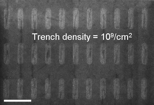
Prior to this, scientists could only place up to several hundred carbon nanotubes at the same time, far from commercialization. IBM used ion exchange chemistry theory to develop a new method that can accurately and controllably place a large number of carbon nanotubes on the substrate in order, the density reached about one billion per square centimeter, which is higher than the previous results. Two orders of magnitude.
IBM first coated carbon nanotubes with a surfactant (thought to make it more water-soluble “soapâ€) and then made substrates with chemically treated hafnium oxide (HfO2) and silica (SiO2). The yttrium oxide is used in the trench, and the substrate is placed in the CNT solution. The nanotubes are chemically bonded to the yttria trench. The rest of the substrate is still “clean†and eventually gets on a single chip. Made tens of thousands of transistors.
Because this method is compatible with standard semiconductor manufacturing processes, large-scale expansion and testing are also simpler.
Of course, this is still the first step in the Long March. Whenever carbon nanotubes can replace silicon, they can only slowly look forward to it.
Ac Motor,12 Volt Fan,Compress Fan,Solar Exhaust Fan
Crown Electronics CO., LTD , https://www.crownelectronicstw.com